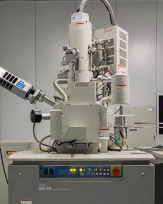
Hitachi Ultra High-Resolution Analytical FE-SEM SU-70
Techniques
SEM, STEM
EDS
Nanolithography System
The SU-70, incorporating Hitachi’s field-proven semi-in-lens technology and a new Schottky electron gun. It features not only ultra-high resolution (1.0 nm/15kV, 1.6nm/l kV), but also reduced charge-up imaging, compositional-contrast imaging, and ultra-low voltage imaging (deceleration mode) derived. Its Schottky electron gun, which can produce probe currents in excess of 200 nA, enables a wide variety of analytical capabilities at high throughput.
Equipment Statistics
| Sample preparation tools | Platinum and gold sputtering system for SEM Carbon evaporator for EDS Small speed diamond SAW for cutting samples |
| Secondary electron image resolution | 1.0 nm @ 15 kV; 1.6 nm @ 1 kV |
| Magnification | 20x - 800,000x |
| Schottky emission gun with probe current | 1 pA - 100 nA |
| 5 axis motor-drive stage | X,Y: 0-110mm, Z: 1.5 - 40mm, Tilt: -5/+70 deg., Rotation: 360 deg. |
| Sample Size | Less than 150mm in diameter |
| Accessories | EDS (EDAX system) NPGS system for e-beam lithography Dedicated back-scattered electron detector STEM |